General Description
The RT6190 is a bidirectal Buck-Boost controller designed for USB power delivery (USB-PD). I It can deliver up to 140W power with maximum 5A current under VOUT = 28V condition with EPC Gallium Nitride FET. This document explains the function and use of the RT6190 evaluation board (EVB) and provides information for the evaluation board schematic, layout, and bill of materials (BOM) to suit individual requirements.
Performance Specification Summary
The RT6190 is a bidirectal Buck-Boost controller designed for USB power delivery (USB-PD) with an input supply voltage range of 4.5V to 36V in a WQFN-40L 5x5 package. The device is mounted on a four-layer evaluation board (EVB) in size of 110mm x 60mm with 1oz copper thickness.
Table 1. RT6190 Evaluation Board Performance Specification Summary
|
Key Features
|
EVB Parameter
|
|
Input Range
|
|
Input Voltage
|
12V to 24V
|
|
Enable Input Voltage
|
2V to 24V
|
|
ALERT Pin Pull-High Voltage
|
1.8V or 3.3V
|
|
Output Range
|
|
Output Voltage
|
5V to 28V
|
|
Maximum Output Current
|
5A
|
|
Maximum Overcurrent Protection
|
6.5A
|
|
Maximum Output Power
|
140W
|
|
Switching Frequency and Package
|
|
Operating Frequency
|
250kHz (typ.) in FCCM
|
|
Package
|
WQFN-40L 5x5
|
Detailed Description of Hardware
Headers Description and Placement
Carefully inspect all the components used in the EVB according to the following Bill of Materials table, and then make sure all the components are undamaged and correctly installed. If there is any missing or damaged component, which may occur during transportation, please contact our distributors or e-mail us at evb_service@richtek.com.
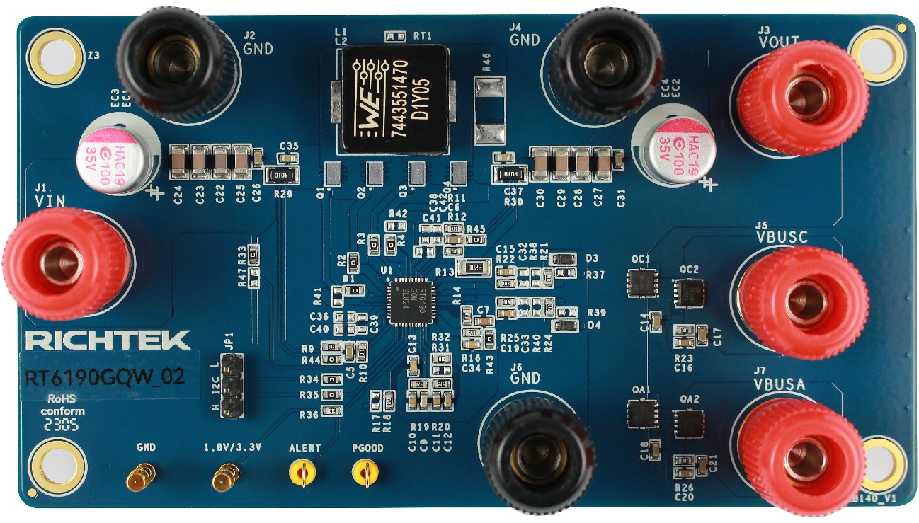
Test Points
The EVB is provided with the test points and pin names listed in the table below.
|
Test Point
|
Pin Name
|
Expected Waveforms or Voltage Levels on Test Points
|
|
J1
|
VIN
|
(1) Positive/Negative terminals for input voltage from power supply to EVB in Forward operation.
(2) Positive/Negative terminals for output voltage from EVB to e-load in Reverse operation.
|
|
J2
|
GND
|
|
J3
|
VOUT
|
Positive terminal for output voltage from EVB to e-load.
|
|
J4
|
GND
|
(1) Negative terminal of output voltage and Power Path C from EVB to e-load in Forward operation.
(2) Negative terminal of input voltage from power supply to EVB in Reverse operation.
|
|
J5
|
VBUSC
|
(1) Positive terminal for Power Path C from EVB to e-load in Forward operation.
(2) Positive terminal for input voltage from power supply to EVB in Reverse operation.
|
|
J6
|
GND
|
Positive/Negative terminals for Power Path A from EVB to e-load.
|
|
J7
|
VBUSA
|
|
JP1
|
I2C
|
Connection for I2C interface.
|
|
GP1
|
1.8V/3.3V
|
External power supply for pull-high voltage of ALERT pin.
|
|
GP2
|
GND
|
Reference voltage for test points.
|
|
TP1
|
PGOOD
|
Test point for PGOOD measurement.
|
|
TP2
|
ALERT
|
Test point for ALERT measurement.
|
Power-up & Measurement Procedure
(1) Forward Operation
- Connect input power supply with wire as wide and short as possible to J1/J2 terminals.
- Connect EN to input voltage though R33, but R47 is NC.
- Connect an external load up to 5A to J4/J5 terminals.
- Set input voltage = 12V and 10A input current limit of input power supply.
- Connect I2C to JP1 pin header, and set register by I2C interface:
- Set 0x0E = 90h to enable RT6190.
- Set 0x29 = 02h to turn on power path C for VBUSC enabled.
- Status check when power on sequence finished:
- VOUT = 5V at J3/J4 terminals.
- VBUSC = 5V at J5/J4 terminals.
- 0x1E = 00h and 0x1F = 40h.
(2) Reverse Operation
- Connect input power supply with wire as wide and short as possible to J5/J4 terminals.
- Connect EN to input voltage though R47, but R33 is NC.
- Connect an external load up to 5A to J1/J2 terminals.
- Set input voltage = 12V and 10A input current limit of input power supply.
- Connect I2C to JP2 pin header, and set register by I2C interface:
- Set 0x0C = 52h for power role swap.
- Set 0x29 = 02h to turn on power path C.
- Set 0x0E = 90h to enable RT6190.
- Status check when power on sequence finished:
- VOUT = 5V at J1/J2 terminals.
- 0x1E = 00h and 0x1F = 40h.
Noticifacation
(1) For other functions, please refer to RT6190 datasheet for detailed description.
(2) The input and output current should not be higher than 9A due to power dissipation of the input and output current sense resistors are all 1W in 1206 size.
Bill of Materials
|
Reference
|
Qty
|
Part Number
|
Description
|
Package
|
Manufacturer
|
|
U1
|
1
|
RT6190GQW
|
Buck-Boost PWM Controller
|
WQFN-40L 5x5
|
Richtek
|
|
L1
|
1
|
7443551470
|
4.7µH/7mΩ/15A
|
12.8x12.8x6.2mm
|
WÜRTH
ELEKTRONIK
|
|
L2
|
1
|
--
|
NC
|
--
|
--
|
|
Q1, Q2, Q3, Q4
|
4
|
EPC2204
|
N-MOSFET for Power Stage (100V/29A)
|
2.5x1.5mm
|
Efficient Power Conversion
|
|
QC1, QC2, QA1, QA2
|
4
|
SM3430NHQA
|
N-MOSFET for USBC/A Power Path (40V/36A)
|
DFN3.3x3.3A-8_EP
|
Sinopower
|
|
D1, D2, D3, D4
|
4
|
1N4148WT-7
|
Diode (100V/0.25W)
(1) External BOOT Voltage for SW1 and SW2
(2) Discharge QC1, QC2, QA1, QA2
|
SOD-523
|
Diodes
|
|
D5, D6, D7, D8
|
4
|
V1P6
|
Schottky Diode (60V/1A)
|
DO-219AD
|
Vishay
|
|
EC1, EC2
|
2
|
--
|
NC
|
--
|
--
|
|
EC3, EC4
|
2
|
350ARHA101M08X8
|
100µF/35V
|
8x3.5mm
|
APAQ
|
|
C3, C4, C34, C35, C37
|
5
|
0603B104K500CT
|
0.1µF/50V/X7R/0603
|
C-0603
|
WALSIN
|
|
C5, C6, C14, C16, C17, C18, C20, C21, C26, C31
|
10
|
GRM188R61H105KAALD
|
1µF/50V/X7R/0603
|
C-0603
|
MURATA
|
|
C7, C8
|
2
|
GRM188R61E475KE11D
|
4.7µF/10V/X5R/0603
|
C-0603
|
MURATA
|
|
C9
|
1
|
0603N1R0C500CT
|
1pF/50V/NPO/0603
|
C-0603
|
WALSIN
|
|
C10
|
1
|
0603B332K500CT
|
3.3nF/50V/X7R/0603
|
C-0603
|
WALSIN
|
|
C11
|
1
|
0603N221J500CT
|
220pF/50V/NPO/0603
|
C-0603
|
WALSIN
|
|
C12
|
1
|
0603B103K500CT
|
10nF/50V/X7R/0603
|
C-0603
|
WALSIN
|
|
C13
|
1
|
0603B333K500CT
|
33nF/50V/X7R/0603
|
C-0603
|
WALSIN
|
|
C15, C19
|
2
|
0603B152K500CT
|
1.5nF/50V/X7R/0603
|
C-0603
|
WALSIN
|
|
C22, C23, C24, C25, C27, C28, C29, C30
|
8
|
1206X106K500CT
|
10µF/50V/X5R/1206
|
C-1206
|
WALSIN
|
|
C32, C33, C36, C38, C39, C40, C41, C42
|
8
|
--
|
NC
|
--
|
--
|
|
R1, R2, R3, R4, R7, R8, R33, R34, R35, R43, R44, R45
|
12
|
WR06X000 PTL
|
0/0603
|
R-0603
|
WALSIN
|
|
R9, R10, R11, R12
|
4
|
WR06X10R0FTL
|
10/0603/1%
|
R-0603
|
WALSIN
|
|
R13
|
1
|
WR12X2200FTL
|
220/1206/1%
|
R-0603
|
WALSIN
|
|
R14, R18, R32
|
3
|
WR06X1003FTL
|
100k/0603/1%
|
R-0603
|
WALSIN
|
|
R15
|
1
|
WR06W1R00FTL
|
1/0603/1%
|
R-0603
|
WALSIN
|
|
R16, R36
|
2
|
WR06X1002FTL
|
10k/0603/1%
|
R-0603
|
WALSIN
|
|
R17, R31, R37, R38, R39, R40, R41, R42
|
8
|
--
|
NC
|
--
|
--
|
|
R19
|
1
|
WR06X4702FTL
|
47k/0603/1%
|
R-0603
|
WALSIN
|
|
R20
|
1
|
WR06X5101FTL
|
5.1k/0603/1%
|
R-0603
|
WALSIN
|
|
R21, R22, R24, R25
|
4
|
WR06X1001FTL
|
1k/0603/1%
|
R-0603
|
WALSIN
|
|
R23, R26
|
2
|
WR06W2R00FTL
|
2/0603/1%
|
R-0603
|
WALSIN
|
|
R29, R30
|
2
|
RLM-1632-6F-R010-FNH
|
10mΩ/1%/1206 for input/output current sense
|
R-1206
|
Cyntec
|
|
R46
|
1
|
--
|
NC
|
--
|
--
|
|
RT1
|
1
|
--
|
NC
|
--
|
--
|
Quick Start with RTMCU WRENBOARD
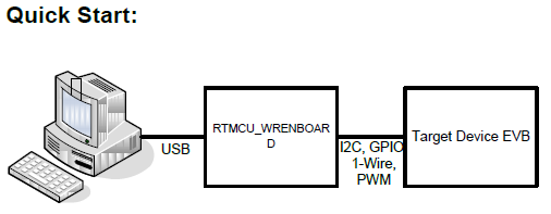
The following summarizes the contents of the Richtek MCU bridge board. In addition to hardware kits, one software utilities is needed to be installed for RTMCU_WRENBOARD bridgeboard.
- Richtek MCU bridge board (RTMCU_WRENBOARD).
- USB B type to micro 5 Pins cable to connect PC and the MCU bridge board. (optional)
- RTBridgeboardUtilities.exe.
RTMCU_WRENBOARD Hardware Description
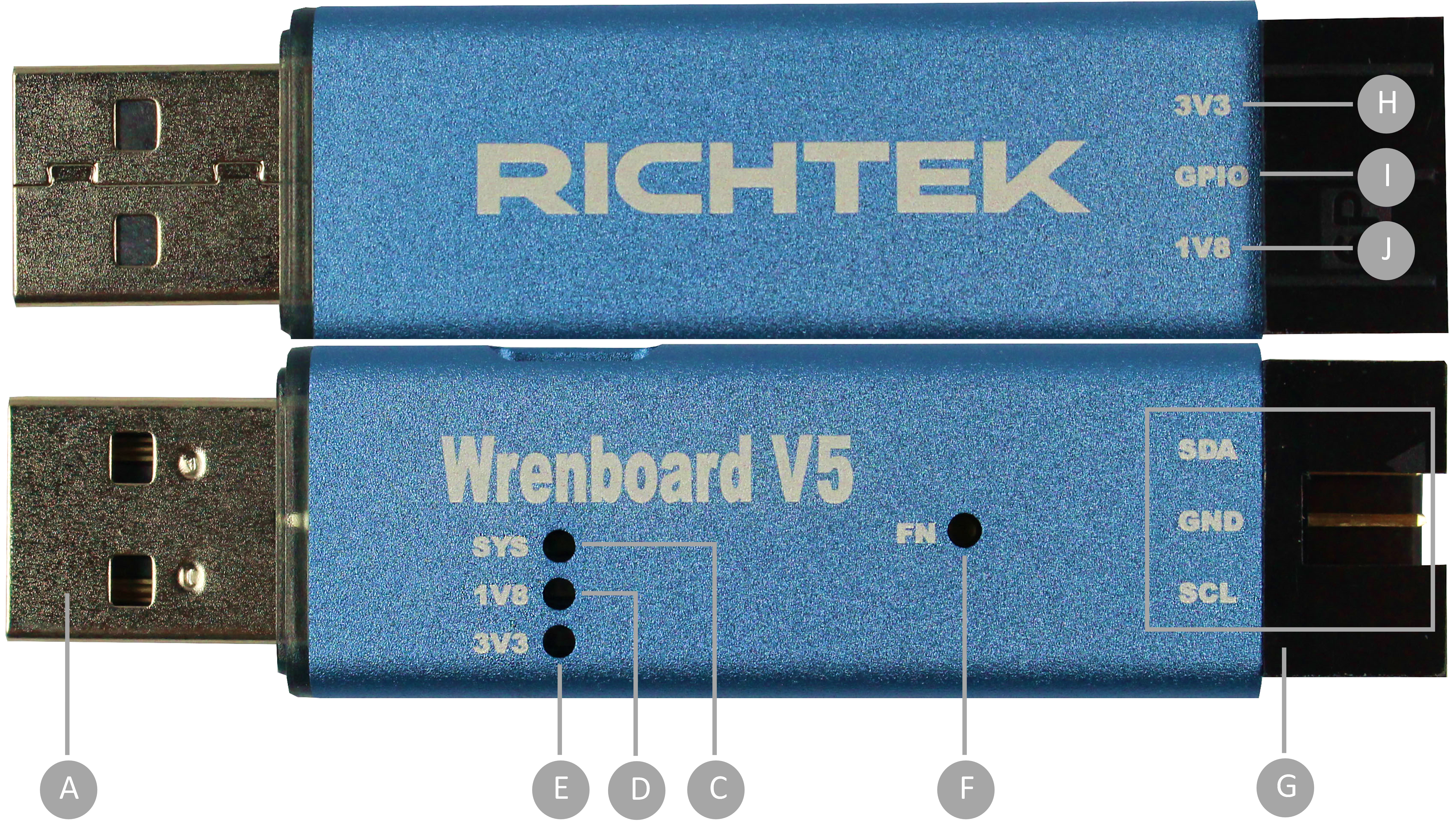
Function Description
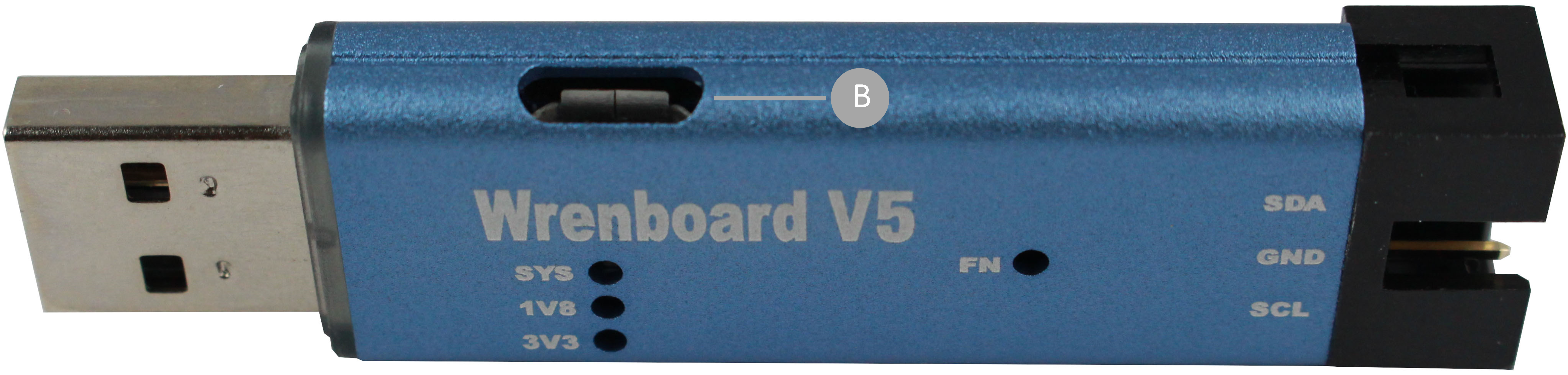
A. Standard USB A plug. It connects to PC directly.
B. Micro 5 pin USB port. It connects to PC by USB cable.
- It is an alternative to connect RTMCU_WRENBOARD to PC when long distance between PC and Device is needed.
C. White LED Indicator
- The white LED indicates RTMCU_WRENBOARD command execution.
D. Blue LED Indicator
- The blue LED indicates I2C (SCL and SDA) are operated in 1.8V.
E. Red LED Indicator
- The red LED indicates I2C (SCL and SDA) are operated in 3.3V.
F. Red LED Indicator. This button has two functions:
- To exchange I2C signals between 3.3V and 1.8V.
- To enable firmware download function.
G. I2C and GND pins
- I2C pins (SDA, GND and SCL) in 3.3V or 1.8V level depend on user setting.
H. Power pins
- Power pins with 3.3V and 1.8V. It is suggested to limit the output current within 100mA for each power pins.
I. GPIO
- User can connect this pin to control device in either function.
The item A/B/C/D/E/G are used for RT6190 EVB.
I2C Control Panel Interface
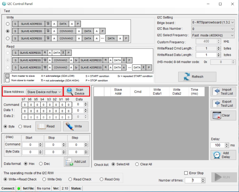
After VIN and EN are ready, and press “Scan Device” button, then “Slave Address” will show 0x2C or 0x2D to indicate RT6190 that can receive I2C command.
Typical Applications
EVB Schematic Diagram
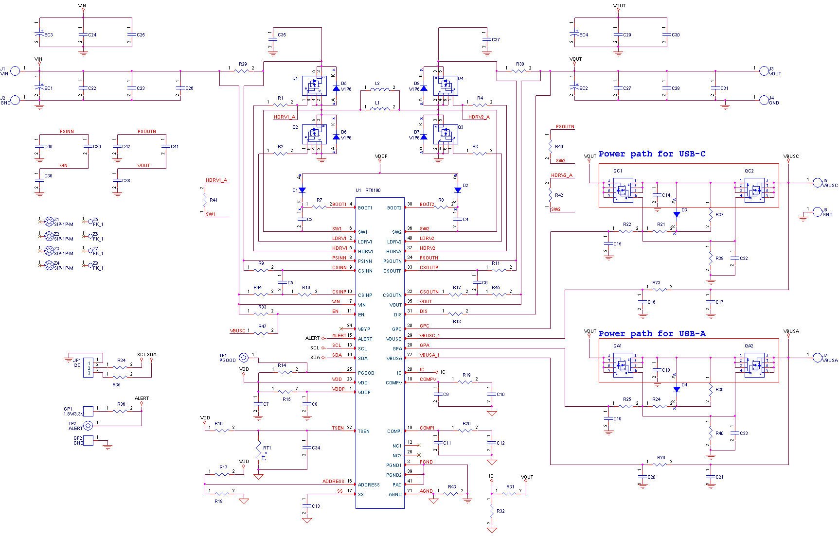
Note:
(1) I2C slave address is 0x2C when R17 = NC, R18 = 100kΩ.
(2) I2C slave address is 0x2D when R17 = 100kΩ, R18 = NC.
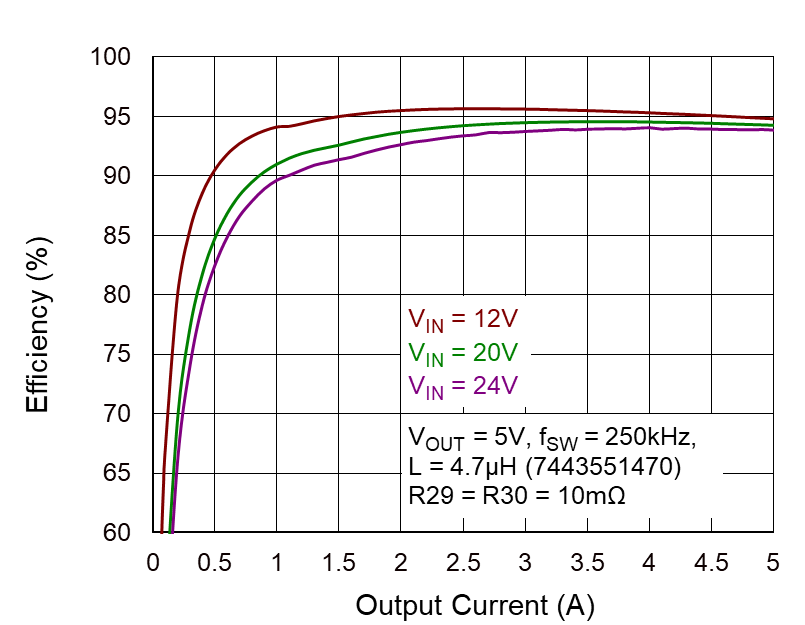
Measure Result
|
Efficiency @ VOUT = 5V
|
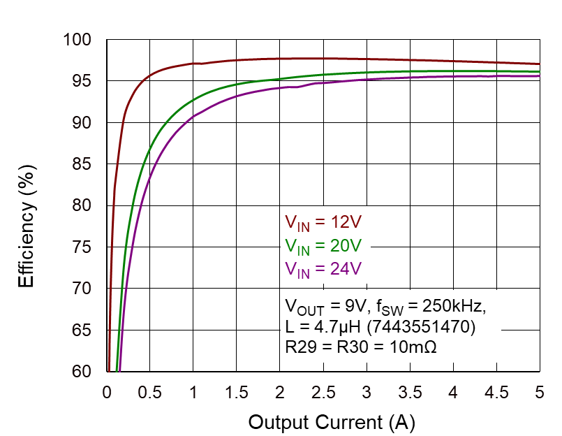
Efficiency @ VOUT = 9V
|
|
|
|
|
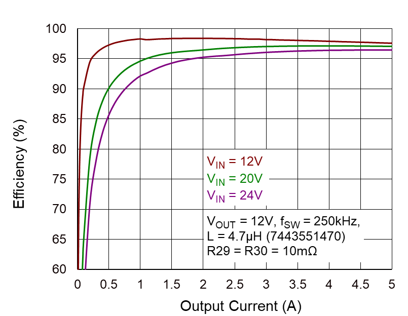
Efficiency @ VOUT = 12V
|
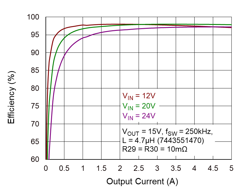
Efficiency @ VOUT = 15V
|
|
|
|
|
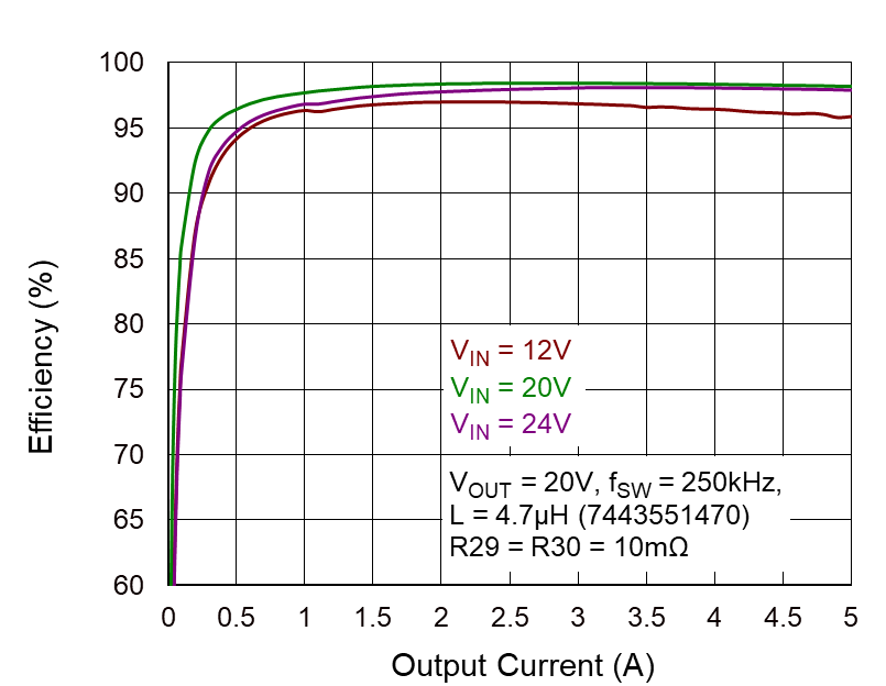
Efficiency @ VOUT = 20V
|
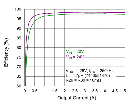
Efficiency @ VOUT = 28V
|
|
|
|
|
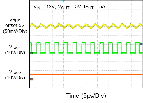
Forward Buck Mode Output Ripple Voltage
|
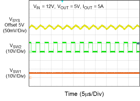
Reverse Buck Mode Output Ripple Voltage
|
|
|
|
|
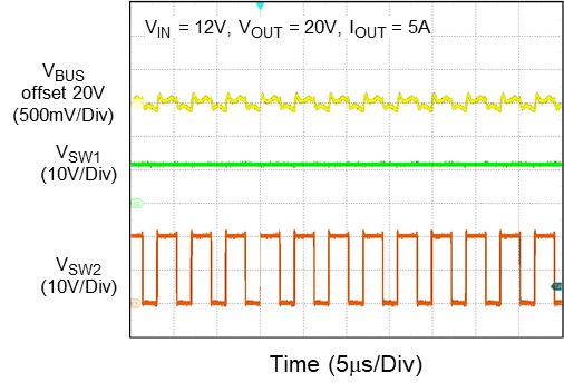
Forward Boost Mode Output Ripple Voltage
|
Reverse Boost Mode Output Ripple Voltage
|
|
|
|
|
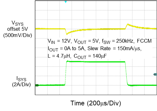
Forward Buck Mode Load Transient Response
|
Reverse Buck Mode Load Transient Response
|
|
|
|
|
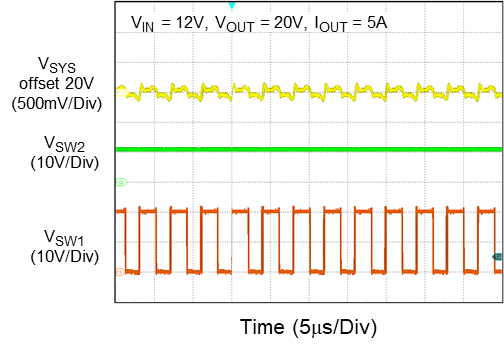
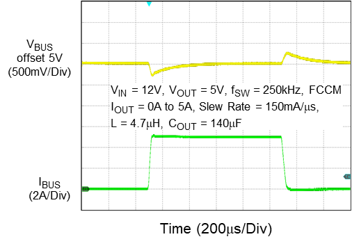
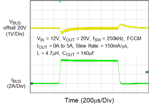
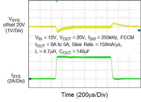
Forward Boost Mode Load Transient Response
|
Reverse Boost Mode Load Transient Response
|
|
|
|
|
|
|
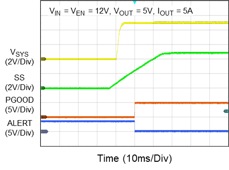
Forward Power-On from I2C
|
Reverse Power-On from I2C
|
|
|

|
|
|
|
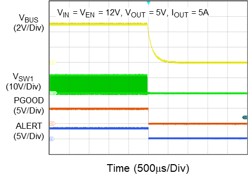
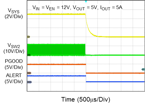
Forward Power-Off from I2C
|
Reverse Power-Off from I2C
|
|
|
|
|
|
Evaluation Board Layout
Figure 1 to Figure 4 are RT6190GQW Evaluation Board layout.
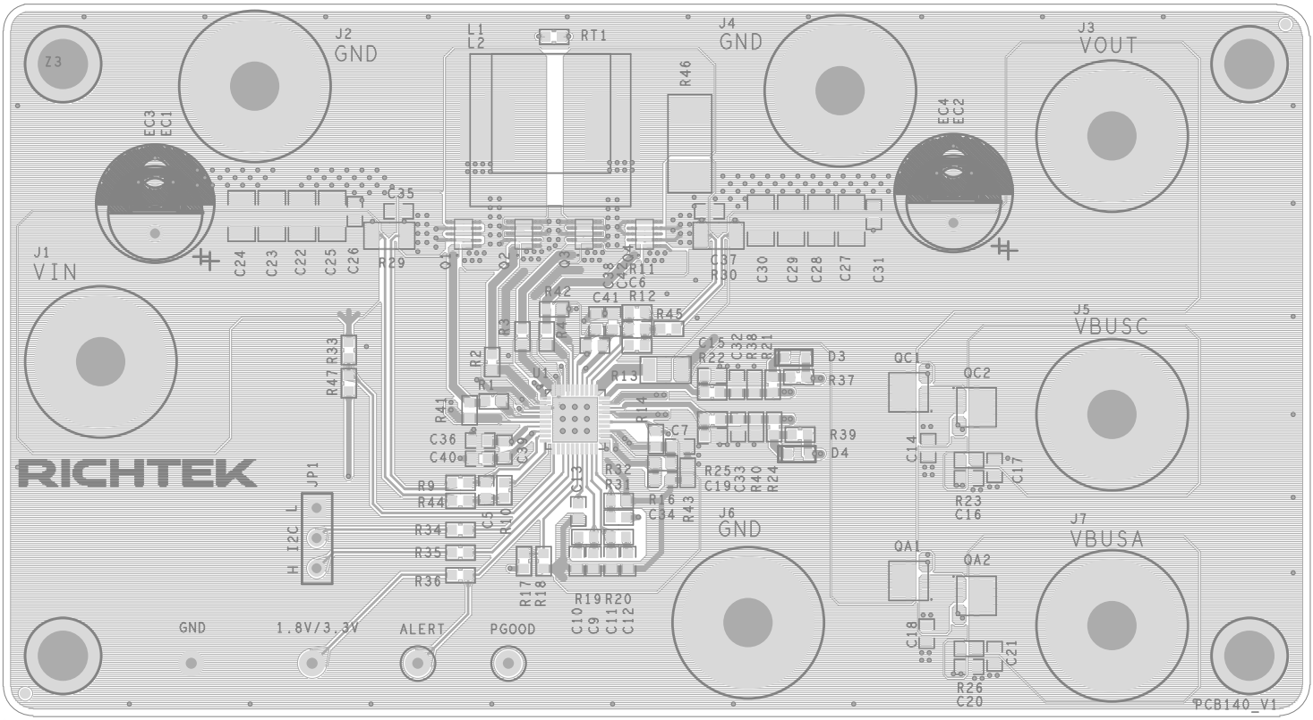
Figure 1. Top View (1st layer)
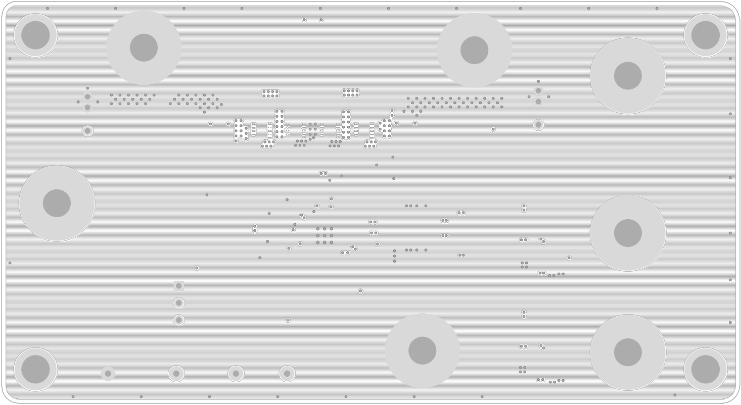
Figure 2. PCB Layout—Inner Side (2nd Layer)
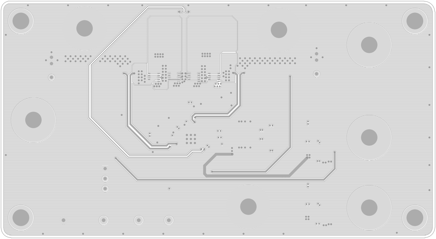
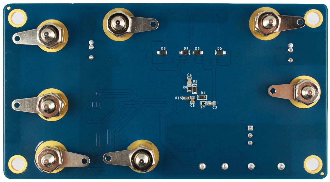
Figure 3. PCB Layout—Inner Side (3rd Layer)
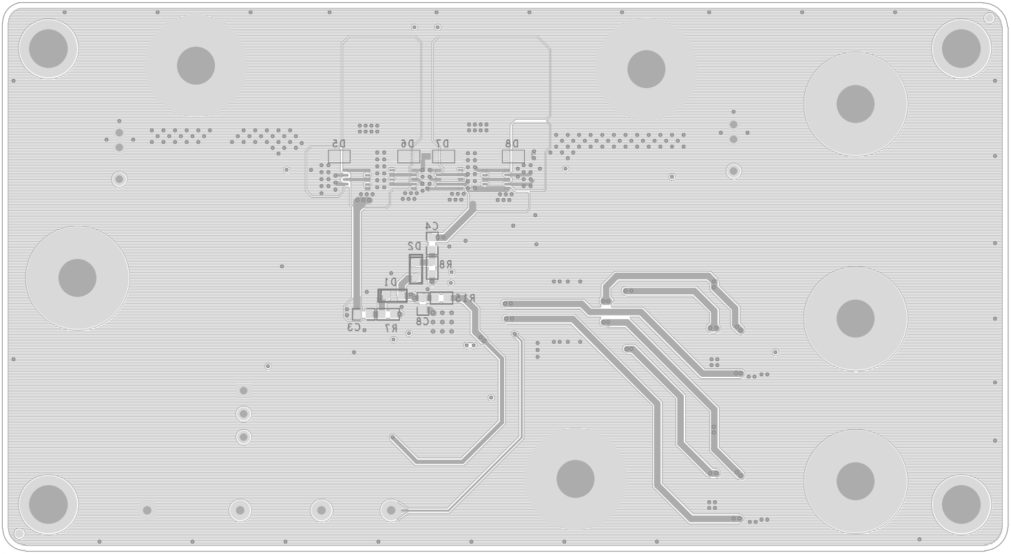
Figure 4. Bottom View (4th Layer)